
8 Layers HDI PCB
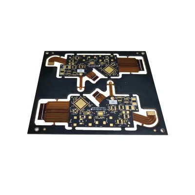
Layers: 8
Surface treatment: immersion gold+OSP
Special process: 2+ HDI
Material: FR4 S1000-2
Line width/line spacing: 3/3mil
Plate thickness: 1.2mm
Copper Thickness: 2Oz
Minimum aperture: 0.10mm
Customer Background
Company Location: Europe
Application: Mobile communications
Field: Communication Equipment
Service: HDI PCB Manufacturing
Project Challenge
The customer certification procedures for high-layer circuit boards are strict and cumbersome, so the entry threshold for high-level circuit boards is relatively high, and the industrialized production cycle is relatively long.
The difficulty is buried vias and plugged vias.
High-level circuit boards have the characteristics of thicker boards, more layers, denser lines and vias, larger unit sizes, and thinner dielectric layers. Inner space, interlayer alignment, impedance control, and reliability requirements are more stringent.
How to Serve
1. Provide free DFM inspection, professional engineers make EQ and working Gerber before production.
2.7*24 hours technical support.
3. A complete HDI equipment production line
4. HDI production is equipped with many professional engineers. Including laser drilling engineers, HDI lamination engineers, HDI full-process process engineers, line engineers, solder mask engineers, and senior engineering R&D personnel.
Results and Benefits
All of the products we produce for our clients are excellent and receive high levels of satisfaction and appreciation from them.
Material thickness and laser drilling are well controlled and meet customer requirements.
Fast delivery wins customers a lot of assembly time.
